Microsoft's Xbox Series X silicon reveal: is this the biggest console processor ever made?
And what does that tell us about its potential power?
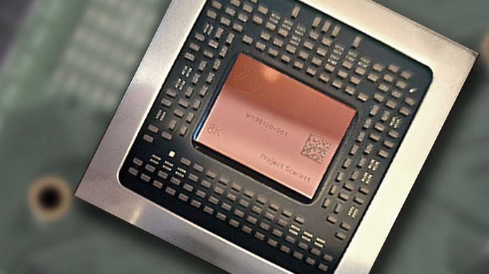
Microsoft's gradual ramp-up to the full reveal of the Xbox Series X continues with Xbox chief Phil Spencer sharing the latest clue towards the technical makeup of the new console. On the face of it, updating a Twitter profile picture with a low quality shot of Project Scarlett silicon might not sound like a big deal - but when Microsoft's stated aim is to deliver the most powerful console of the next generation, commentators (including us!) will grab every opportunity we can to learn more about the new machine. And the evidence does suggest that we're looking at the largest console processor released by Sony or Microsoft to date, further solidifying expectations of extreme performance.
Actually getting any kind of meaningful measurement from this latest controlled leak from Microsoft isn't easy. Perhaps purposefully so, the image is of a low resolution, taken at an angle and with a curious lens distortion effect. The measurement of silicon area is important though - we can safely assume that the Scarlett processor is fabricated with the same 7nm lithography as AMD's latest Zen 2 and Navi chips - the core building blocks at the heart of this year's wave of new consoles. Stacked up against AMD parts using the same production techniques, we can get some idea of the scale of its graphics core.
Ascertaining the size of Microsoft's chip gives us some idea of its architectural makeup - but more than that, area on a microprocessor isn't cheap. Every square millimetre adds to build cost and it has to count. Yes, comparisons against new AMD parts could be valuable, but comparing chip measurements with prior console generations also gives us some idea on just how much investment Microsoft is sinking into this new console - and by extension, how much it'll cost to build and how much we may end up paying for it.
Since Phil Spencer's initial tweet, senior director of Xbox hardware David Prien has also weighed in with a further shot of the new processor. Since Spencer himself is already in possession of a fully armed and operational Series X console, these processor samples are likely 'wastage' from the production line - chips with defects that didn't pass QA. These aren't much use in getting working consoles out of the door, but clearly they're powerful conversation pieces! Again, the new photograph is taken from an angle but that hasn't stopped online commentators including myself from taking a shot at getting an area measurement!
Prior attempts at doing so - from the Project Scarlett E3 2019 reveal trailer - revealed a processor with area in the region of 380mm2. Compared to Xbox One X, this would represent a 5.8 per cent increase in size which stacks up on top of the move from a 16nm to 7nm production process - so we have more transistors packed onto the die, and more area to play with on top of that. However, recent leaks and messaging from Microsoft (not to mention the sheer size of the Series X casing) suggest an absolute beast of a machine, with a mooted 12 teraflops of compute power. Fragments of specs from a recent AMD testing leak also suggest that the Series X chip features 56 compute units. While this leak is far from conclusive, again, it points towards a chip of unprecedented size.
All of which has resulted in various online commentators looking at the photos of the Scarlett chip with an almost forensic level of analysis. Lens distortion and perspective correcting filters in Photoshop can reformat the Microsoft images into a traditional 'top down' image, and measurements can be calculated. However, what is needed is a point of comparison in the real world to scale things accurately.
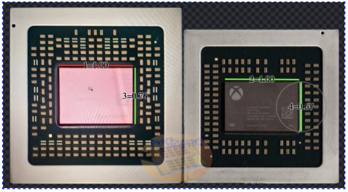
To begin with, I envisioned the Scarlett processor as being mounted within the same 50mm square package that surrounded Xbox One X's Scorpio engine. However, once the new chip was scaled accordingly, it quickly became clear that the area of the processor was now lower than Xbox One X, at around 90 per cent of the size. A chip of this area likely wouldn't require the extraordinary form factor of the Series X casing, so I needed to rethink.
Other real world counterparts on the chip are there, however. The surface-mounted components that surround the processor tend to be a standard size and in this case, they seem to be the same dimensions as those found on Xbox One X. It's from here where Wccftech produced an eminently reasonable die size estimate, suggesting an approximate 401mm2. This would represent an 11.7 increase in area from Xbox One X, making it by far the largest console processor ever made - to the best of my knowledge, at least.
Some ambiguity remains, of course. Fundamentally, measurements are being derived from a low quality, low resolution image pushed through untold Photoshop filters. This may explain why other commentators used the distance between the surface-mounted components as a basis for measurement. Personally, I thought I'd try a hybrid approach - using both pitch and component-size, scaling the image until components in all corners of the image would line up when the Scarlett processor was overlaid onto the Xbox One X chip. My result is 405mm2, so just a touch larger than Wccftech's estimate - almost 13 per cent larger than the Scorpio engine. A compelling analysis on Reddit from user _rogame based on the later, much higher quality David Prien image gives an broadly equivalent result - 407mm2.
The next question is obvious: does this result add anything to the leaks we've already seen - or does it discount them? The fundamental building blocks of Zen 2 and Navi at 7nm are known and we have several examples of them to work from. The Radeon 5700XT delivers 40 compute units and a bunch of on-die features that are likely to make their way into consoles - and the AMD Navi 10 GPU here consumes 250mm2 of area. An octo-core Zen 2 CPU set-up with interconnectivity 'glue' and reduced L3 cache compared to desktop equivalents would likely come in at around 65mm2. Combining these two crucial elements together and delivers a prospective processor similar in size to PS4 Pro, which used a 325mm2 chip on the older 16nm fabrication process. In turn, the original PlayStation 4 delivered 348mm2 at 28nm.

| Processor Size | Process Node | Compute Units/TFLOPs | CPU Architecture | |
|---|---|---|---|---|
| Xbox Series X | Circa 405mm2 (unconfirmed) | 7nm | 56/12TF (unconfirmed) | Zen 2 |
| Xbox One X | 359mm2 | 16nmFF | 40/6TF | Jaguar |
| PlayStation 4 Pro | 325mm2 | 16nmFF | 36/4.2TF | Jaguar |
| PlayStation 4 'Slim' | 208mm2 | 16nmFF | 18/1.84TF | Jaguar |
| PlayStation 4 | 348mm2 | 28nm | 18/1.84TF | Jaguar |
| Xbox One S | 240mm2 | 16nmFF | 12/1.4TF | Jaguar |
| Xbox One | 363mm2 | 28nm | 12/1.31TF | Octo-Core Jaguar |
Assuming the 400+mm2 measurement holds true for Xbox Series X, that's a whole lot of extra area - easily enough to contain the big increase in shader count that the recent AMD testing leak hints at. It's also worth remembering that Xbox Series X has confirmed hardware-based features that are not present in existing AMD Navi-based graphics cards - ray tracing and VRS support, for example - which are likely to have some bearing on the physical size of the Scarlett processor.
Of course, stepping back for a moment and playing Devil's advocate on our own analysis, the fact is that we are drawing a lot of conclusions from images that have been warped, twisted and resized in ways that some consider to be unnatural - but while I had some reservations and doubts about my own Photoshopping skills, the results and methodology of the Reddit post stand up well to scrutiny. The precise measurements of the Project Scarlett chip will likely be revealed in concert with the final specification of the machine - as was the case with Xbox One X - but in the here and now, it's job done for Microsoft: the excitement level continues to move upwards and Xbox Series X looks even more beastly than previously envisaged.
Perhaps I'm being ever-so-slightly cynical here but I'd say that controlled releases like this from Microsoft are designed very much to engender this sort of discussion and debate - and I guess it works! The conclusion I draw from this latest phase of the process only serves to hammer home what I thought about the Series X reveal last month. What we understand as the traditional limitations of console design are being redefined for next-gen. Microsoft wants the highest performing box, so the processor is the largest, most transistor-dense design it could come up with - and this in turn requires a bigger box and innovation in how to handle thermal dissipation. But equally, doubling down on pushing back barriers also prompts questions about how much this machine costs to build and how much Microsoft will charge for it. While spec reveals can't be too far away, the chances are we'll have to wait until E3 or beyond for the specifics on the costs of next-gen hardware.


